
STMT12-BD
12-Inch Large-Platform Wafer Inspection Microscope
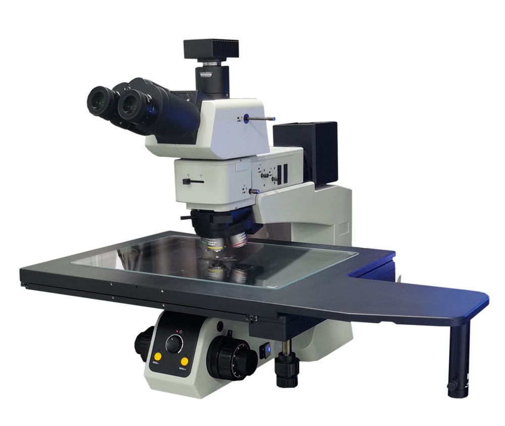
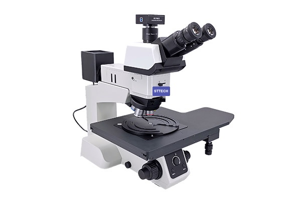
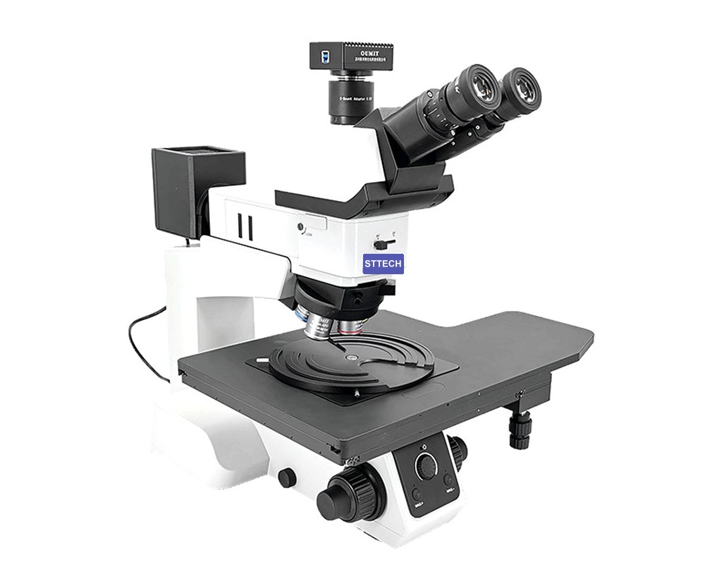
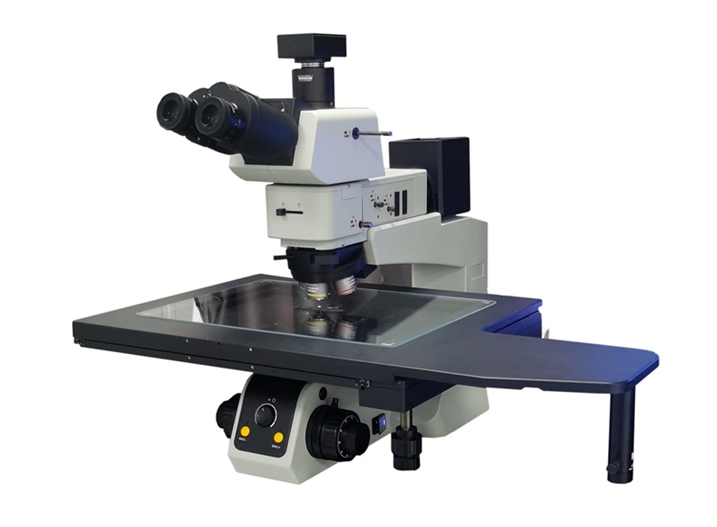
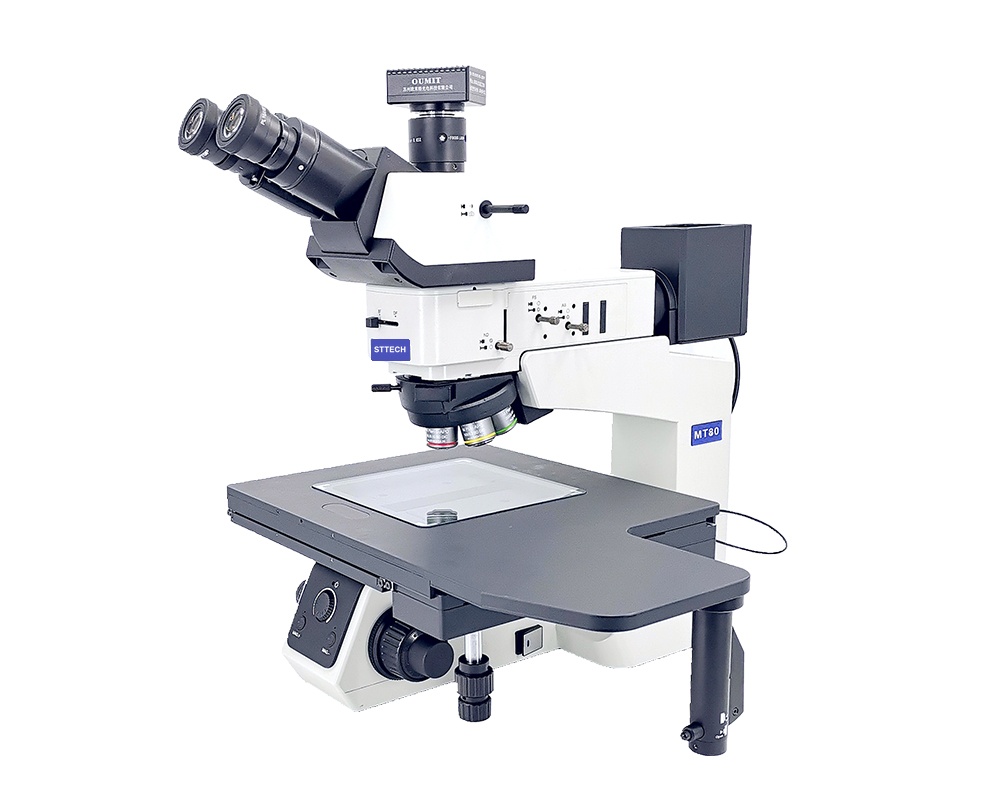
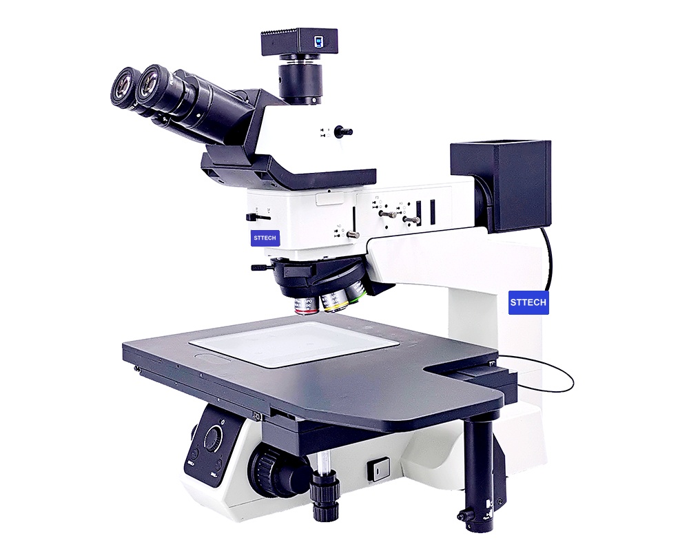
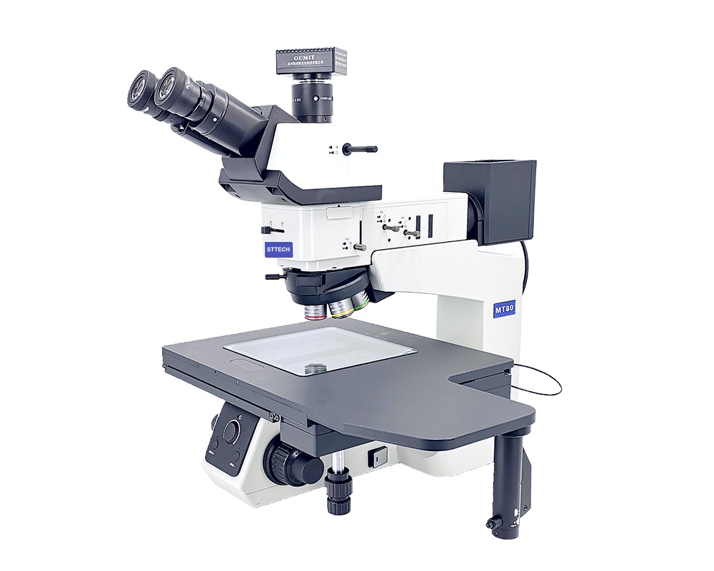
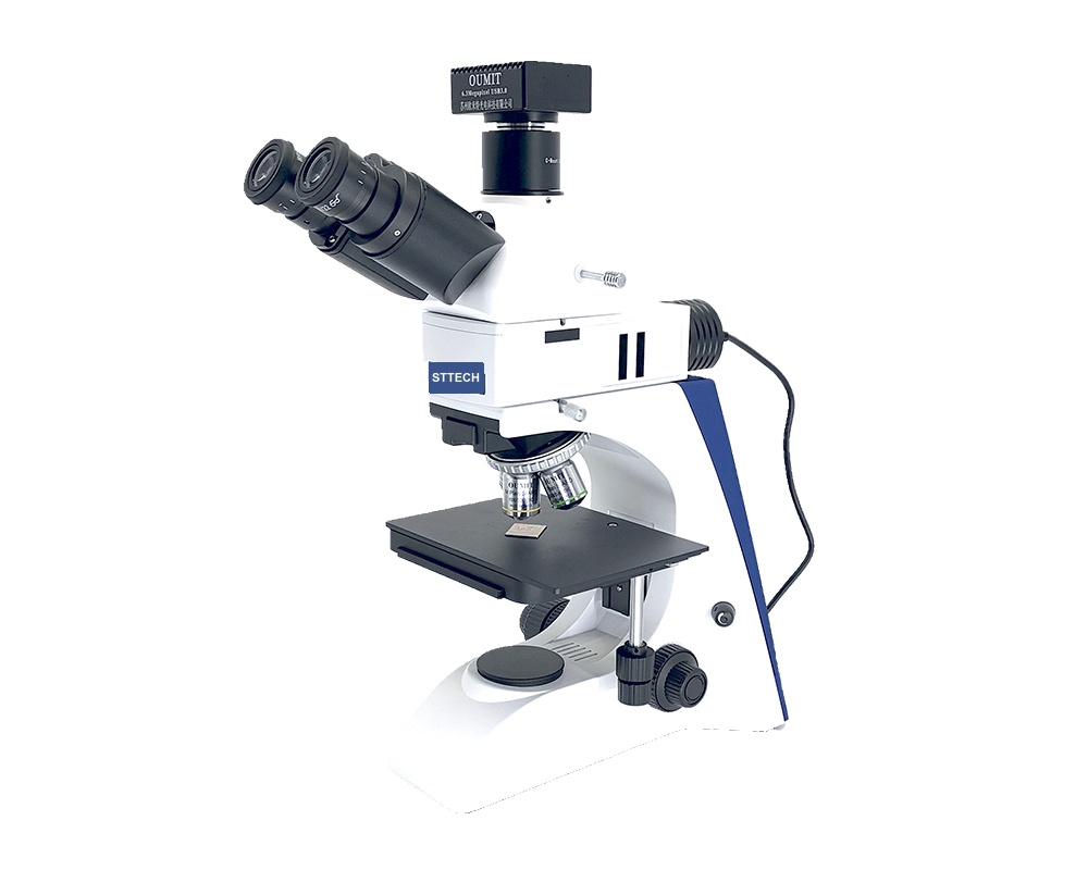
STMT12-BD is a large-platform semiconductor wafer inspection microscope built on infinity color-corrected optics. The 710 × 420 mm mechanical stage with 356 × 305 mm X-Y travel handles 12-inch wafers, photomasks, oversized panels and large workpieces — while bright/dark-field illumination, a coded BD turret and ST-1.5D software deliver defensible, measurable images from 50× to 3000×.
Key Features
Infinity BD Optics
Long-working-distance bright/dark-field semi-apochromat objectives 5×–50× standard, up to 1000× with the optional 100×.
12-Inch X-Y Platform
710 × 420 mm table with 356 × 305 mm travel, coaxial X-Y controls and quick-release for whole-wafer navigation.
Coded BD Nosepiece
5-position turret with DIC slot; magnification and calibration values follow automatically in the software — no measurement errors from forgotten recalibration.
Motorized Turret Option
Motorized BD turret controlled from both the physical button and the software for fully repeatable workflows.
ST-1.5D Software
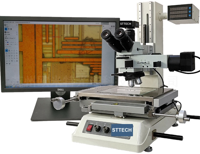
Capture, measurement, barcode upload, live image stitching and extended depth of focus in one workflow.
Polarizing Ready
Polarizer slider and 360° rotating analyzer for stress birefringence and anisotropic materials.
Specifications
| Model | STMT12-BD |
|---|---|
| Stage | 14″ platform, 710 × 420 mm table with 356 × 305 mm X-Y travel, coaxial control with quick-release |
| Optical system | Infinity color-corrected optical system |
| Optical magnification | 50× – 500× (1000× optional) |
| Digital magnification | 150× – 1500× (21.5″ monitor); up to 3000× with 100× objective |
| Camera | 12 MP 1/1.8″ Sony color industrial sensor (6.3 MP / 20 MP optional) |
| Observation head | Tiltable trinocular head, erect image, interpupillary 50–76 mm, 100:0 photo tube split |
| Eyepieces | High-eyepoint widefield SWH10X/25 mm, focusable |
| Objectives | Infinity long-working-distance BD semi-apochromat: 5× NA0.15 WD15 · 10× NA0.30 WD8.4 · 20× NA0.40 WD11.9 · 50× NA0.75 WD3.0; optional 100× NA0.90 WD1.0; optional plan-apochromat BD 50× NA0.55 WD8.0 / 100× NA0.80 WD2.8 |
| Nosepiece | BD 5-position turret with DIC slot — coded turret synchronizes magnification and calibration with the software; motorized turret with dual software / button control (optional) |
| Stand | Transmitted & reflected stand, low-position coaxial coarse/fine focusing, 35 mm coarse travel, 0.001 mm fine, tension adjustment and upper travel stop |
| Condenser | Swing-out achromatic condenser N.A. 0.9 |
| Reflected illuminator | Bright/dark-field illuminator with aperture and field diaphragms, centerable, filter slot and polarizer/analyzer slots |
| Illumination | 10 W adjustable LED, transmitted & reflected, pre-centered |
| Camera port | 0.65× C-mount adapter, focusable (0.5× / 1× optional) |
| Polarizing kit | Polarizer slider, 360° rotating analyzer slider |
| Computer | Brand PC and monitor included |
| Software | ST-1.5D measurement software — motorized turret control, capture, video, measurement, barcode upload, live image stitching and extended depth of focus |
| Stage micrometer | Precision stage micrometer, 0.01 mm graduation |
System Views
Application Gallery
Applications
Semiconductor & Wafer Inspection
Wafer surface defects, process layers, photoresist and packaging inspection on wafers up to 12 inches.
Metallography & Quality Control
Microstructure analysis, grain size and coating thickness of metals, alloys and coatings under bright/dark field.
Electronics & Materials Research
PCB, solder joints, IC packaging, ceramics and composites — with polarizing kit for anisotropic materials.
Request a Quote
Tell us your wafer size and inspection requirements — we will configure the right STMT system and provide a demo scan with your own specimens.